Solution Overview
With the widespread adoption of smart devices and the continuous evolution of fast-charging protocols, consumer demand for power adapters has fully upgraded from ‘just being able to charge’ to ‘fast charging, multi-port, portable, and safe.’ In the highly competitive fast-charging market, how can a brand create products with differentiated competitiveness? A high-performance multi-port charger power supply customization solution—covering everything from the underlying architecture to the industrial design—is the key to achieving product breakthroughs.
I. Core Pain Points and Customization Advantages
Conventional multi-port chargers on the market today commonly face several pain points: rigid power distribution when multiple ports output simultaneously (often causing devices to disconnect and restart), severe heating under high power, and bulky dimensions that hinder portability.
Through deeply customized solutions, we can fundamentally solve these problems and deliver the following core values to our customers:
-
Precise Power Distribution Strategy: Customized intelligent dynamic power allocation algorithms tailored for different scenarios (e.g., ultrabook + phone + watch).
-
Ultimate Power Density: By leveraging cutting-edge semiconductor materials and topologies, we achieve power output of over a hundred watts in an extremely compact form factor.
-
Unique Brand Visuals: From housing molds and ventilation hole array design to silk-screen customization, everything perfectly aligns with the brand identity.
II. Core Technology Architecture: The Foundation of High Efficiency
An excellent internal electrical architecture is the top priority when building a high-performance, high-power multi-port charger. For customized requirements in power ranges from 65 W to 240 W and even higher, the solution is deeply optimized at the fundamental technical level:
1. The Golden Combination: PFC + LLC Resonant Converter
To meet stringent energy efficiency standards while shrinking the form factor, customized solutions typically adopt the industry-leading topology of an active PFC (Power Factor Correction) stage combined with an LLC resonant converter.
-
PFC Stage: A carefully designed PFC inductor working with high-efficiency switching transistors not only effectively improves the power factor and reduces grid harmonic pollution but also provides a stable DC bus voltage for the downstream stage.
-
LLC Stage: Leveraging LLC resonant soft-switching technology (ZVS/ZCS), switching losses are minimized, significantly boosting overall conversion efficiency (up to 93% and above). This is the core enabler for achieving high power density and superior thermal management.
2. Deep Application of Gallium Nitride (GaN) and Silicon Carbide (SiC)
By introducing third-generation wide-bandgap semiconductor materials and exploiting their high-frequency, high-voltage, and high-temperature characteristics, the size of passive components such as transformers and capacitors is further reduced, breaking through the physical limitations of traditional silicon-based materials.
3. Intelligent Multi-Port Dynamic Power Distribution
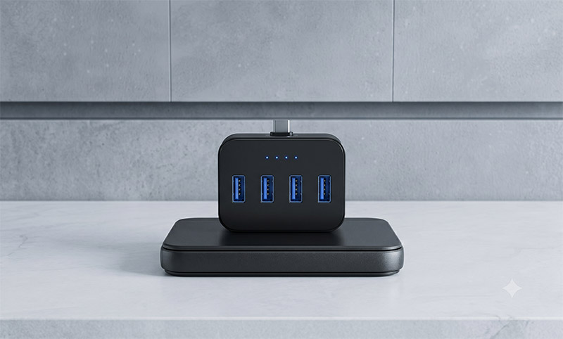
A built-in high-performance MCU protocol chip supports mainstream fast-charging protocols such as PD3.1 (EPR), PPS, and QC. When multiple devices are connected simultaneously, the main control chip dynamically reallocates power among the ports (e.g., 2C1A, 3C1A, 4C configurations) on a millisecond-level basis according to the handshake protocol and battery status of each device, eliminating frequent disconnections and delivering a seamless charging experience.
III. Structural and Thermal Management Design: Uniting Safety and Aesthetics
The byproduct of high power density is heat. In the customization of multi-port chargers, thermal management directly determines product safety and lifespan.
-
Customized Ventilation Hole Array and Housing Structure: In addition to using internal materials such as high-thermal-conductivity potting compounds and graphene heat-spreading sheets, we can also carry out professional industrial design for the housing. For example, a specifically patterned geometric ventilation hole array not only physically creates effective air convection channels to accelerate heat dissipation but also serves as a distinctive product visual signature (ID design).
-
Rigorous Safety Protection: The solution integrates comprehensive OVP (Over-Voltage Protection), OCP (Over-Current Protection), SCP (Short-Circuit Protection), and OTP (Over-Temperature Protection) to ensure the safety of both the power supply and the connected devices under all extreme operating conditions.
IV. From R&D to Mass Production: End-to-End Full-Chain Enablement
A mature customization solution is not just a design on paper, but also represents reliable manufacturing and delivery capabilities:
-
Requirement Analysis and Prototype Design: Based on the customer’s interface requirements (number of Type-C/Type-A ports), total power requirements, target audience, and cost budget, we provide a preliminary technical specification.
-
PCBA Development and Debugging: Senior power engineers carry out schematic design, PCB layout, and in-depth optimization of PFC magnetics and LLC transformer parameters.
-
Safety Certification and Testing: We assist in completing major global safety and environmental certifications such as CCC, CE, FCC, RoHS, and UL, ensuring compliant entry into international markets.
-
Standardized Manufacturing: Relying on a well-established supply chain and a strict quality control system (AOI, ATE automated testing, burn-in rooms, etc.), we ensure that every batch of delivered power supply products exhibits extremely high consistency and reliability.